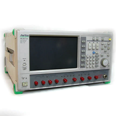
|
Carrier frequency
|
Frequency range
|
300 kHz to 2250 MHz (MG3670B/C), 300 kHz to 2750 MHz (MG3671A/B)
|
|
Accuracy
|
Depends on installed reference oscillator*1
|
|
Internal reference oscillator
|
Frequency: 10 MHz
Start-up characteristics: ≤1 x 10⁻⁷/day (after 30-min. warm-up), ≤5 x 10⁻⁸/day (after 60-min. warm-up) Aging rate: ≤2 x 10⁻⁸/day (after 24-h warm-up)
Temperature characteristics: ≤±5 x 10⁻⁸ (0˚ to 50˚C)
|
|
External reference input
|
10 MHz or 13 MHz (±10 ppm), 2 to 5 Vp-p, BNC connector (rear panel)
|
|
Reference output
|
10 MHz, 2 to 5 Vp-p, BNC connector (rear panel)
|
|
Output
|
Level range
|
–143 to +13 dBm (resolution: 0.1 dB)
|
|
Frequency response
|
≤±1 dB (at 0 dBm output)
|
|
Level accuracy
|
Output level/frequency
|
≤1000 MHz
|
>1000 MHz
|
|
–33 to +13 dBm
|
±1 dB
|
±2 dB
|
|
–123 to –33.1 dBm
|
±1.5 dB
|
±2 dB
|
|
–136 to –123.1 dBm
|
±3 dB
|
±4 dB
|
|
Impedance
|
50 Ω, N-type connector
|
|
Continuously variable level
|
Continuously variable output over 20 dB range (+8 to –12 dB) in 0.1 dB steps within upper and lower limits of any output level
|
|
Level unit
|
dBm, dBµ, µV, mV, V (dBµ, µV, mV, V selected terminate/open voltage display)
|
|
Interference radiation
|
≤1 µV *Measured 25 mm from cabinet (except rear panel) with two-turn 25 mm diameter loop antenna, terminated with 50 Ω load, ≤+5 dBm output, carrier wave
|
|
Signal purity
|
Spurious
|
≤–65 dBc (≥100 kHz offset, ≤±100 MHz bandwidth), ≤–50 dBc (≥100 kHz offset, full band),
≤–40 dBc [spurious of (5.4–Fout) GHz at ≥2.65 GHz], ≤–30 dBc (harmonics)
|
|
SSB phase noise
|
≤–120 dBc/Hz (100 kHz offset, carrier wave)
|
|
Digital modulation
|
Internal modulation
|
Depends on installed modulation unit (MG0301C/0302A/0305A/0307A/0310A/0311A/0312A)
|
|
External modulation
|
Any modulation using I/Q input signal Input frequency: DC to 1.2 MHz*2
Input level: √ I2 ± Q2 ≤0.5 Vrms, BNC connector *I/Q ≤1.5 Vp-p (50 Ω), I/Q ≤10% to 100% of 1.5 Vp-p (CMOS) Vector error: ≤1.8%rms (I/Q input level: 1 Vrms/50 Ω, at ≤+5 dBm output)
|
|
I/Q output
|
Outputs I/Q signal at internal modulation (MG0301C/0302A/0305A/0307A/0310A/0311A/0312A installed)
|
|
Pulse modulation
|
Input
|
TTL level, BNC connector, polarity selectable
|
|
On/off ratio
|
≥40 dB (at ≥0 dBm output)
|
|
Transition time
|
≤2 µs, minimum pulse width: 10 µs
|
|
Memory function
|
Frequency memory
|
1000 carrier frequencies (save and recall)
|
|
Parameter memory
|
100 panel settings (save and recall)
|
|
Other functions
|
Relative display
|
Carrier frequency, output level
|
|
I/Q signal adjustment
|
Offset, balance, phase (only output) of I/Q input/output signal
|
|
Backup
|
Last settings stored at power-off
|
|
Reverse power protection
|
Maximum reverse input power: 50 W (<1000 MHz), 25 W (≥1000 MHz), ±50 V (DC)
|
|
GPIB
|
All functions except power switch and panel lock switch controlled Interface function: SH1, AH1, T6, L4, SR1, RL1, PP0, DC1, DT0, C0, E2
|
|
Operating temperature
|
0˚ to 50˚C
|
|
Power
|
100 to 120/200 to 240 Vac (switchable), 47.5 to 63 Hz, ≤550 VA
|
|
Dimensions and mass
|
(426±5) W x (221.5±4) H x (451±5) D mm, ≤27 kg
|
|
EMC
|
EN55011: 1991, Group 1, Class A
EN50082-1: 1992
|
|
Safety
|
EN61010-1: 1993 (Installation Category II, Pollution Degree II)
|


)
)
)
)
)
)
)
)
)
)
)
)
)
)
)
)
)
)
)
)